
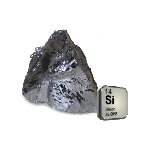
Polysilicon is made from silica sand. The world produces tens of millions of tons of metal-grade polysilicon and metallurgical-grade polysilicon every year, of which less than 5% of metallurgical-grade polysilicon is purified into electronic-grade polysilicon with a purity level of 12N or above. SEMI M16 and JEITA EM-3601A both regulate the shape, size, purity, surface metal contamination, appearance and packaging of polysilicon. We mainly explain the aspect of "surface metal contamination" of polysilicon blocks.
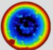
When there is metal contamination on the surface of polycrystalline silicon blocks, these contaminated blocks will cause deep-level defects during the process of melting in the crystal growth furnace, growing crystal rods, and turning into IC components, which is harmful to the application of IC components (such as causing leakage, etc.). Therefore, after the crystal rods are produced, they will be monitored to confirm whether the crystal rods are contaminated with metal. Due to the characteristics of crystal rod growth, metal contamination is often found on the periphery of the crystal rod in a donut shape (as shown in the red area on the right).
Due to the limitation of detection technology, the pollution monitoring at this stage can only clearly know the degree of iron pollution, but not other metal pollution; this detection technology is limited to crystal rods with resistance greater than 1 ohm, and is not applicable to crystal rods with resistance less than 1 ohm. Therefore, we should advance the monitoring time to the inspection of polycrystalline silicon blocks before feeding: before feeding production, first confirm the metal pollution of polycrystalline silicon blocks to ensure the quality of crystal rods.
There is a real case to share: When a crystal growth plant introduced the second source, it evaluated the products of a polysilicon manufacturer in a certain country. During the early evaluation of the material blocks, it was found that the metal concentration on the surface of the polysilicon was higher than that of the original material blocks used. In the subsequent trial production, it was found that the performance of the wafers produced was not as good as the original material blocks used in the test. Finally, it was determined that the polycrystalline material blocks produced by this manufacturer could not be used. Such early detection and verification avoided unnecessary subsequent cost losses, including lengthy verification time and waste of defective crystal rod output.
So how do we detect the surface metal of polycrystalline silicon blocks? ICP-MS can be a good solution. First, we need to prepare the following reagents:

The operation process is as follows:
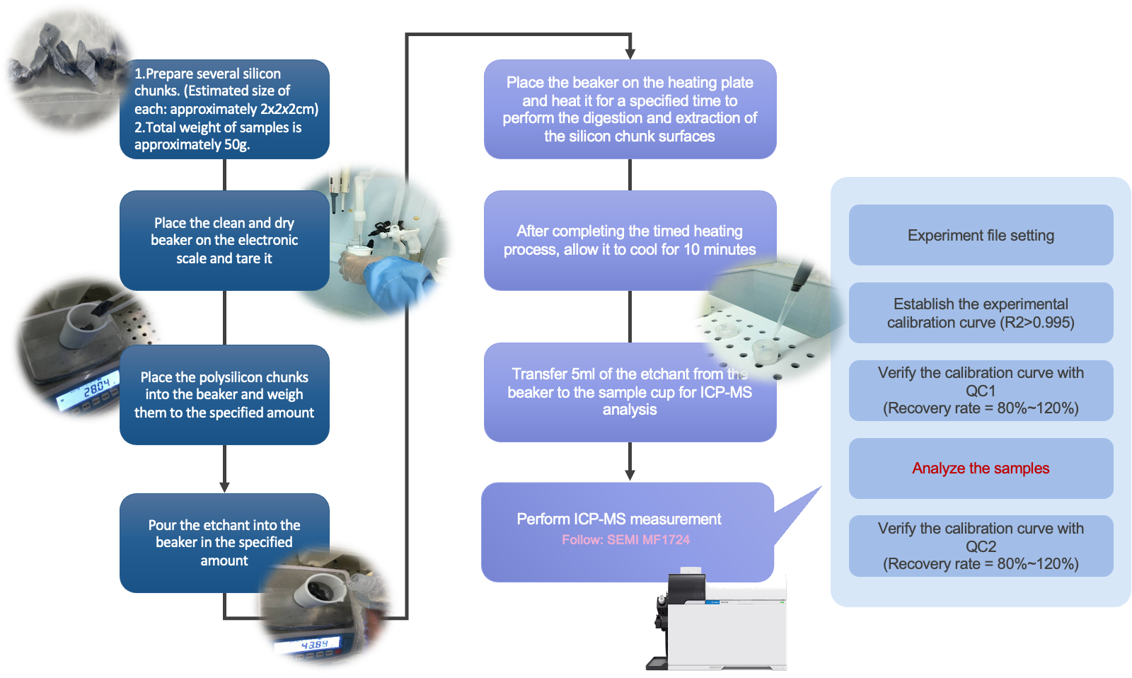
Finally, a complete data report can be produced for customer reference.
The cost (including manpower and materials) of each crystal rod from the beginning to the completion of growth is very huge. If it is not carefully monitored in the early stage, once metal contamination abnormalities occur due to raw materials, it will cause great losses.
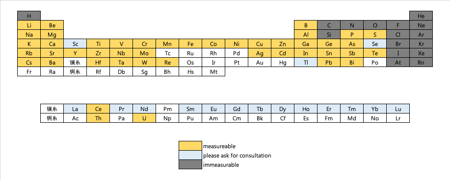
Shangwei Technology can provide customers with more than 40 element test results (as shown in the table below) to help customers obtain more complete information; if you have the need for metal element inspection and analysis of raw materials, please contact us!
 Inquiry mailbox x