Material analysis and inspection play an extremely important role in the manufacturing and production process and are crucial to ensuring product quality, improving production efficiency and meeting customer needs.
MSP team and partners can assist customers in the following material analysis or monitoring. Whether in the semiconductor industry or other industries, quality control or process capability improvement can be achieved through analytical services.
In addition, the company continues to plan and build various measurement resources, and can also provide various measurement resource inquiry and delivery services.
In modern scientific research and industrial applications, precise elemental analysis is a key technology. Inductively coupled electromagnetic mass spectrometry (ICP-MS) is receiving more and more attention as an advanced technology with high sensitivity, high resolution and the ability to analyze multiple elements simultaneously.
The analysis process of ICP-MS is to introduce the sample to be measured in the form of an aqueous solution into a high-temperature argon plasma through atomization to generate ions. These ions then enter the vacuum system, pass through the quadrupole column and detector, and the element is confirmed and its concentration is quantified by mass-to-charge ratio and ion number.
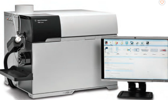
Shangwei Technology has considerable experience, and the ICP-MS machine is highly sensitive and precise, and can conduct comprehensive analysis of various substances. Our measurement services cover water quality, wafers, O-ring seals, various powder materials, etc. Whether it is the detection of trace elements or complex sample analysis, we can provide professional and reliable support to help you gain in-depth understanding. Composition and quality of materials.
Currently, the Agilent7900 owned by Shangwei Technology can detect a wide range of elements, from 6 to 260 amu (Li to U), a total of 68 elements. If you have special element requirements, customers are also welcome to contact us; in addition, the analysis range of ICP-MS is from ppt to ppm level, ensuring extremely high detection sensitivity.
During the analysis process of ICP-MS, we use
Our laboratory environment is a CLASS100 clean room; the clean room provides an air particle environment that is better than the industry. Such an environment has the following advantages:
We are a laboratory that has passed the ISO/IEC 17025:2017 international certification, which ensures that every test has a standard process from beginning to end; the standard procedure for ICP-MS measurement operations As follows:
/投影片2.JPG)
After completing the analysis, we will produce a detailed and complete data report for customer reference; we also promise to provide a feedback time that is better than the industry to make customer projects progress more smoothly and efficiently .
Our professional team can also assist with in-depth data statistical analysis to ensure accurate and reliable results and help customers make the best decisions quickly.
In addition, Shangwei has recently added a high-performance microwave digester, which will significantly improve the pre-treatment capabilities of ICP-MS, especially in sample digestion, enabling it to more efficiently process samples of various complex matrices; we will also provide commissioned testing services in more areas. [Please refer to Microwave Digester for details]
 In order to ensure the accuracy of analysis results, customers are kindly requested to pay attention to the following points when providing samples :

If you want to know more, please feel free to contact us!
ICP-MS technology has demonstrated its unparalleled advantages in elemental analysis and plays an indispensable role in both scientific research and industrial applications. Shangwei Technology is committed to providing the most advanced ICP-MS analysis services and looks forward to cooperating with you to jointly explore the mysteries of trace elements.
Contact window | 徐先生 Jack Hsu
email: jackhsu@msp-sw.com tel: 03-4884766
 @102dgxnw
A flexible single quadrupole ICP mass spectrometer that provides the industry's best matrix tolerance, most efficient helium collision mode, lowest detection limits and widest dynamic range.
ICP-MS stands for Inductively Coupled Plasma Mass Spectrometry (Inductively Coupled Plasma Mass Spectrometry), which is a highly sensitive and high-resolution analytical technology mainly used to determine the presence and concentration of elements.
The principle of ICP-MS is based on the sample being injected into an inductively coupled plasma to form a high-temperature plasma. The energy in this plasma is enough to ionize the atoms in the sample. The ionized atoms are separated and detected by a mass spectrometer, and based on their mass/charge ratio, the presence and concentration of the element can be determined.
Reference: www.agilent.com
High sensitivity
ICP-MS has extremely high sensitivity and can detect very low concentrations. Element, the widest dynamic range in quadrupole ICP-MS, providing up to 11 orders of magnitude dynamic range, from ppt levels to hundredth-level concentrations.
High Resolution
Due to the use of a mass spectrometer, ICP-MS has high resolution, making it Able to distinguish between different elements of very close mass.
Multi-element analysis
ICP-MS can measure multiple elements simultaneously, which makes it possible to It is widely used in analytical applications in various fields, such as environmental monitoring, biomedical research, food testing, etc.
Quick Feedback
ICP-MS 7900 has ultra-fast data acquisition function and can complete 10,000 data per second independent measurements
Can provide quantitative analysis and in-depth analysis of trace elements and impurities; mainly semiconductor materials, including metal and dielectric materials. Detection can provide information on elemental composition and chemical structure. Extensible for analyzing insulating and biomedical materials.
Secondary Ion Mass Spectrometry (SIMS) is a highly sensitive surface analysis technology that is often used in fields such as semiconductors, materials science, life sciences, and geology. SIMS can provide very detailed information on the elemental composition and chemical structure of the surface.
High spatial resolution
SIMS has a very high spatial resolution, which can reach sub-micron or The smaller scale allows for high-precision analysis of tiny areas.
High sensitivity
SIMS is capable of detecting elements at very low concentrations, typically in parts per million to a concentration range of 1 part per billion.
Surface composition analysis
SIMS is mainly used for surface analysis, so it can analyze the composition and structure of the material surface. Details are provided.
It can analyze the surface morphology and physical properties of materials, sample hardness and other mechanical quality testing of materials.
AFM stands for Atomic Force Microscope and is a high-resolution microscope that has many uses. It is a powerful tool that plays an important role in nanoscale research and applications in various fields, including materials science, biology, nanotechnology, etc.
Patented Technology
Dimension Edge uses Bruker's patented PeakForce Tapping ® technology to provide the best-in-class products in its class. High level of atomic force microscope performance and functionality.
Widely used
Corresponding experimental plans can be formulated according to different research directions, and it has advanced Nanoscale measurement capabilities.
Accurate measurement
Features low drift and low noise, improving data acquisition speed and reliability sex. Its integrated visual feedback and pre-configured settings make it like an expert operating on-site, with highly consistent measurement results.
This device combines the functions of an optical microscope, a scanning electron microscope and a surface roughness meter
Laser Scanning Conjugate Microscope (LSCM) is an advanced optical imaging technology that provides high resolution, high contrast and real-time observation capabilities, making it an ideal choice for materials science in various fields. or an indispensable tool in fields such as biological sciences.
Scan system
LSCM consists of a scanning system that uses lenses or prisms to direct a laser beam as it moves across the surface of the sample. Through rapid scanning of fixed-point light sources, LSCM can construct high-resolution images in three-dimensional space.
Confocal technology
By using confocal technology, the system ensures that only light from the focal plane passes through the detector, thereby eliminating scattered light from other parts of the sample. This improves the contrast and resolution of the image.
3D imaging
Due to the characteristics of the scanning system, LSCM can acquire images at focal planes at different depths. This allows researchers to construct highly detailed three-dimensional sample structures.
High-end equipment for material analysis, used in advanced materials science, scientific and industrial thin film technology, semiconductor process development and other fields, can be used to study and analyze crystal structure, crystal phase, lattice parameters, crystal size, etc.
High-end equipment for material analysis is used in advanced materials science, scientific and industrial thin film technology, semiconductor process development and other fields. It can be used to study and analyze the measurement of crystal structure, crystal phase, lattice parameters, crystal size, etc.
The X’Pert3 MRD Series offers advanced features and performance, making it an important analytical tool in materials science. Here are some of its main features:
Semiconductors and monocrystalline wafers
Whether used for growth research or device design, the process of using high-resolution XRD to measure structural layer quality, thickness, stress, and alloy composition has become an important part of electronic and optoelectronic multilayer The core of research and development of semiconductor equipment.
With a wide selection of X-ray mirrors, monochromators and detectors, the X'Pert3 MRD and MRD XL offer high-resolution configurations to suit different material systems - from lattice-matched semiconductors, to delayed buffer layers , to new foreign layers on non-standard substrates.
Polycrystalline Solids and Thin Films
Whether used for growth studies or device design, the process of using high-resolution XRD to measure structural layer quality, thickness, stress, and alloy composition has become an important part of electronic and optoelectronic multilayer The core of research and development of semiconductor equipment.
Polycrystalline layers and coatings are an important component of many thin film and multilayer devices. The evolution of polycrystalline layer morphology during deposition is a major research area in the development of functional materials.
X'Pert3 MRD and X'Pert3 MRD XL can be fully equipped with a series of incident light path components such as slit systems, parallel X-ray mirrors, polycapillary lenses, cross slits and single capillaries for reflection Rate, stress, texture and phase identification tests to make selections.
Ultra-thin films, nanomaterials and amorphous layers
Functional devices may contain disordered, amorphous or nanocomposite films. The flexibility of the X'Pert3 MRD and MRD XL systems allows the combination of multiple analytical methods.
A range of high resolution optics, slit and parallel plate collimators are available to achieve optimal performance for grazing incidence, in-plane diffraction and reflectivity testing.
Measurement under non-temperature conditions
Studying how materials change under various conditions is an important part of materials research and process development.
The X’Pert3 MRD and MRD XL are specifically designed to easily integrate with Anton Paar’s DHS1100 non-temperature sample stage, enabling automated measurements over a range of temperature ranges and inert gas environments.
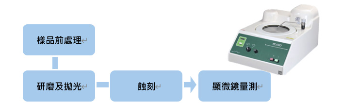
The amount of damage layer removal is an item that must be carefully evaluated in the manufacturing process. Too much removal will result in reduced production and increased costs; but too little removal will result in extremely high processing fragments or defects. Risks; in order to solve such problems, we can detect the depth of the damaged layer through effective analysis methods, so that the back-end process can adjust the accurate removal thickness.
The amount of damage layer removal is an item that must be carefully evaluated in the manufacturing process. Too much removal will result in reduced production and increased costs; but too little removal will result in extremely high processing fragments or defects. Risks; in order to solve such problems, we can detect the depth of the damaged layer through effective analysis methods, so that the back-end process can adjust the accurate removal thickness.
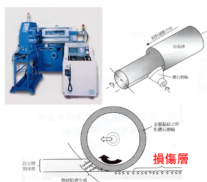
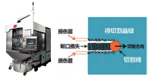
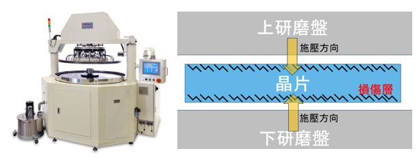
During the wafer manufacturing process, from grinding the outer diameter of the crystal rod, slicing the crystal rod, to grinding the wafer, the crystal rod and the wafer will be damaged by external forces, which is the so-called damaged layer (Damaged layer) on the surface of the crystal rod and the wafer. Layer); if the damaged layer is not properly removed, there is a high chance that the chip will break or form defects in subsequent processes, thus affecting the yield.
Therefore, the amount of damage layer removal is an item that must be carefully evaluated in the manufacturing process. Too much removal will result in reduced output and increased costs; but too little removal will result in extremely high processing fragmentation. Or the risk of defect formation, affecting the overall yield.
In order to solve this problem, we can detect the depth of the damaged layer through effective analysis methods, so that the back-end process can adjust the accurate removal thickness.
Damage layer often occurs in:
Crystal rod outer diameter grinding machine: The damage layer appears on the outer diameter of the crystal rod after grinding;
Ingot slicing machine: Damage layer appears on both sides of the wafer;
Wafer grinder: Damage layer appears on both sides of the wafer.
Ingot outer diameter grinding machine
Ingot slicing machine
Ingot slicing machine
After the final etching of the sample, the damaged layer can be clearly observed, defined and measured under a microscope. By calculating the measured values, the true depth of the damaged layer can be obtained for customer reference.
| Sample | 8 inches<100> | Process site | Grinding |
| Photos | 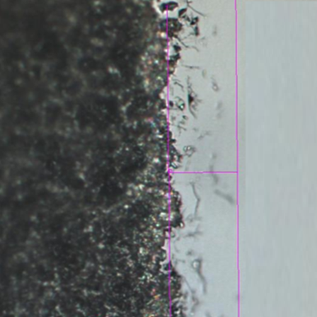 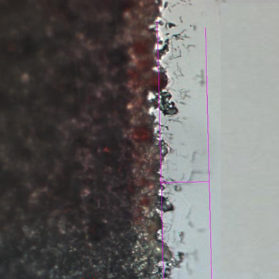 |
||
| Sample | 8 inches<100> | Process site | slice |
| Photos | 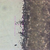 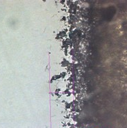 |
||
| Sample | 6 inches<100>Nitrogen doped | Process site | Grinding |
| Photos |   |
||
| Sample | 6-inch <100> crystal rod | Process site | Outside diameter roller grinding |
| Photos | 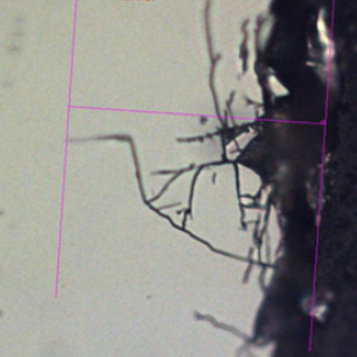  |
||
Advanced microwave digestion system, suitable for sample pretreatment, such as digestion. Can be widely used in environmental analysis, food testing, pharmaceuticals, materials science and other fields.
Microwave digestion is a highly efficient sample pretreatment technology that accelerates sample dissolution and digestion through high temperature and pressure, shortens sample pretreatment time and reduces contamination risk for subsequent elemental analysis (such as ICP-MS or ICP-OES).
We are very happy to introduce that Shangwei has recently added a high-performance microwave digester, which will significantly improve our pre-treatment capabilities for various samples, properly handle challenges from different customers, and enable it to process various complex samples more efficiently; we will also provide more commissioned testing services in more fields, including but not limited to the following:
Our advantages are:
✅ High efficiency: Our digestion system has high throughput processing capabilities and can process multiple samples at the same time, which can significantly shorten the pre-processing time by more than 50%, allowing you to get your test results faster!
✅ High functionality: High temperature and pressure processing up to 250°C & 40 bar ensures complete digestion of even the most difficult metal, ceramic or organic samples, providing more accurate analysis results.✅ Low contamination: The closed processing system can reduce the risk of sample loss and contamination.
✅ Intelligent system: Real-time pressure monitoring, automatic container locking, touch interface and preset digestion methods can ensure consistent test conditions each time, greatly reduce variables, ensure stable and error-free analysis process, and make your test results more reliable.
If you have any commissioned testing needs, please contact us directly and we will do our best to serve you!


 ▲ Reciprocal space exploration
 ▲Swing Curve analysis
 ▲Structural Analysis
  ▲Reflectance
  ▲Grazing incident phase identification
 ▲ internal diffraction
 ▲Peak height changes with temperature and time

 Inquiry mailbox