
In our damage layer detection and analysis service, we have introduced the damage layer analysis process and detection methods for crystal rods and wafers. This article will further explain in detail the damage layer detection technology of silicon electrode columns.
As shown in the figure below (Figure 1), this is the object of our observation this time - the silicon electrode column. From the picture, we can clearly see the holes, grooves and cutting marks left on the surface after drilling and processing, and these locations are all areas where the damaged layer may appear (Figure 2).
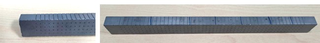
Figure 1. Silicon electrode column
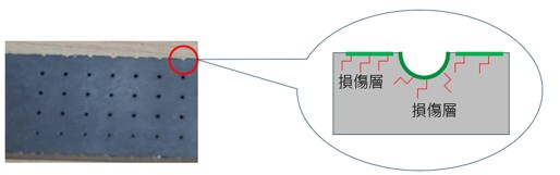
Figure 2: Schematic diagram of the damaged layer
Silicon electrode column is a columnar silicon material made through high-precision processing and is often used in electrochemical devices, energy storage devices, or semiconductor-related components. They are often designed to be porous and have high surface area to increase conductivity or reactive surface area.
During the processing, mechanical actions such as cutting and drilling can easily cause damage to the surface or subsurface structure, such as microcracks, plastic deformation or amorphization. These damaged areas are called damage layers.
On the surface of silicon electrode pillars, the damage layer is commonly found in the following areas:
If these damages are not discovered early, they may affect the subsequent process yield, conductivity performance, and even reduce the product life.
To observe these damaged layers, we need to first segment the sample appropriately (Figure 3), cut the area to be observed into appropriate sizes, and then follow the following steps (Figure 4):
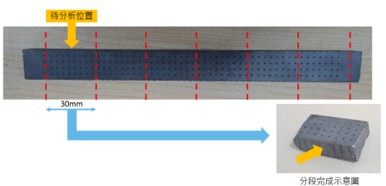
Figure 3: Segmented work
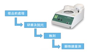
Figure 4. Operation Procedure
After processing, damage layers with depths ranging from tens to hundreds of microns can be observed in areas such as the grooves (Figure 5). When observed from the side, the thickness and range of the damaged layer can also be clearly identified (Figure 6).
These analyses help determine the effects of machining on the material, thereby improving process parameters or preventing defects.
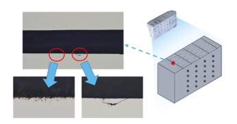
Figure 5. Groove damage layer
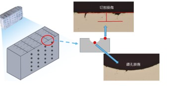
Figure 6. Side analysis of damage
 Inquiry mailbox x